LVDS PCB Layout Guidelines: Optimize Your Design! pcb design tutorial: basic rules, tips and guidelines-techsparks
If you are searching about PCB Design Review and Layout Clean-Up | Sierra Circuits you've came to the right place. We have 25 Images about PCB Design Review and Layout Clean-Up | Sierra Circuits like Some LVDS PCB Layout Guidelines For Ensuring Signal, 40% OFF, Some LVDS PCB Layout Guidelines For Ensuring Signal, 40% OFF and also Component Placement in PCB Design & Assembly | Sierra Circuits. Here it is:
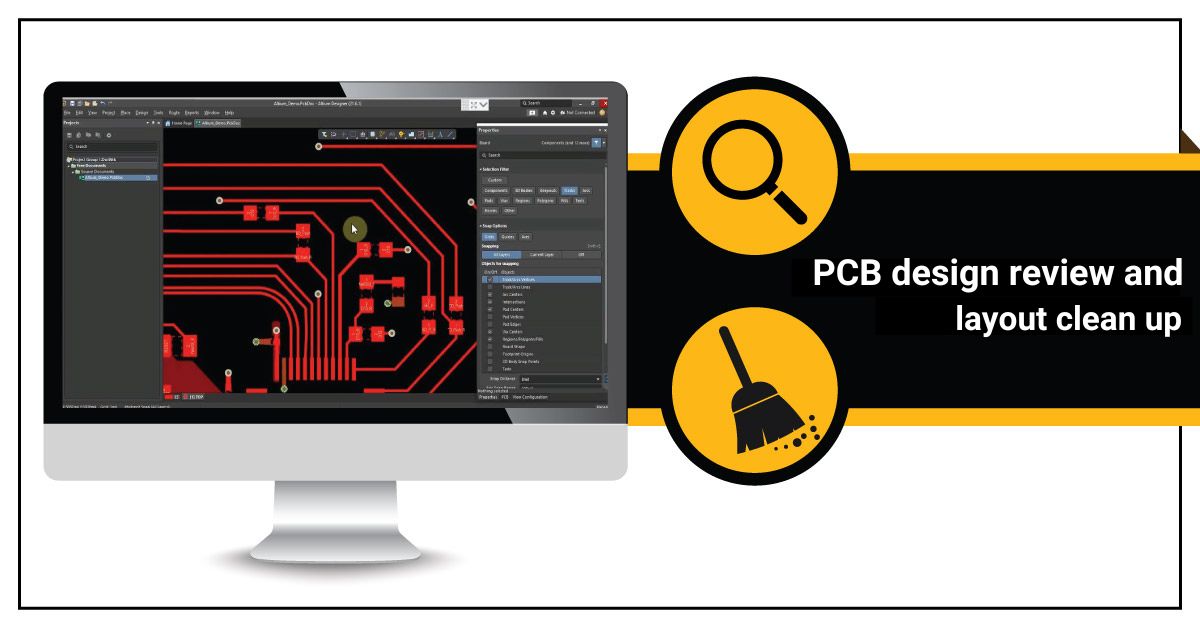
PCB Design Review And Layout Clean-Up | Sierra Circuits
 www.protoexpress.com
PCB Design Review and Layout Clean-Up | Sierra Circuits
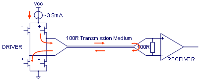
LVDS-PCB-Layout-Guidelines Für Gute Signalintegrität | Altium
LVDS-PCB-Layout-Guidelines für gute Signalintegrität | Altium
LVDS PCB Layout – Expert Guidelines You Need To Know! Pcb Layout Design
 superspotsz.blogspot.com
LVDS PCB Layout – Expert Guidelines You Need to Know! Pcb layout design ...
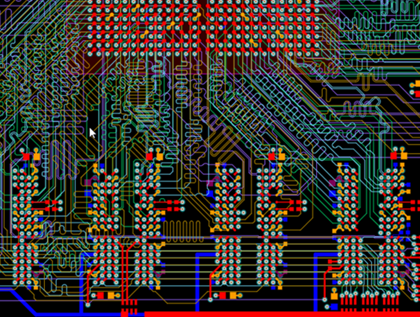
Main Design Guidelines & Layout Rules On High Speed PCB
 www.integrasources.com
Main Design Guidelines & Layout Rules on High Speed PCB
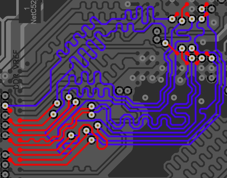
PCB Routing Guidelines For DDR4 Memory Devices And Impedance | Blog
 resources.altium.com
PCB Routing Guidelines for DDR4 Memory Devices and Impedance | Blog ...
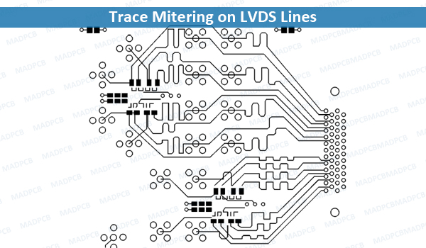
Some LVDS PCB Layout Guidelines For Ensuring Signal Integrity | PCB
 resources.altium.com
Some LVDS PCB Layout Guidelines for Ensuring Signal Integrity | PCB ...
Main Design Guidelines & Layout Rules On High Speed PCB
 www.integrasources.com
Main Design Guidelines & Layout Rules on High Speed PCB
Some LVDS PCB Layout Guidelines For Ensuring Signal, 40% OFF
 www.oceanproperty.co.th
Some LVDS PCB Layout Guidelines For Ensuring Signal, 40% OFF
Component Placement In PCB Design & Assembly | Sierra Circuits
 www.protoexpress.com
Component Placement in PCB Design & Assembly | Sierra Circuits
Some LVDS PCB Layout Guidelines For Ensuring Signal Integrity | PCB
 resources.altium.com
Some LVDS PCB Layout Guidelines for Ensuring Signal Integrity | PCB ...
Grounding Pcb Crystal Layout Electrical Engineering S - Vrogue.co
 www.vrogue.co
Grounding Pcb Crystal Layout Electrical Engineering S - vrogue.co
Main Design Guidelines & Layout Rules On High Speed PCB
 www.integrasources.com
Main Design Guidelines & Layout Rules on High Speed PCB
24. Top 5 PCB Design Guidelines Every PCB Designer Needs To Know,PCB Design
 www.juvtmall.com
24. Top 5 PCB Design Guidelines Every PCB Designer Needs to Know,PCB Design
PCB Design Tips | Circuit Board Layout & Design Guidelines
 www.wellpcb.com
PCB Design Tips | Circuit Board Layout & Design Guidelines
Main Design Guidelines & Layout Rules On High Speed PCB
 www.integrasources.com
Main Design Guidelines & Layout Rules on High Speed PCB
Understanding LVDS Interface: A Comprehensive Guide
 www.shiningltd.com
Understanding LVDS Interface: A Comprehensive Guide
Main Design Guidelines & Layout Rules On High Speed PCB
 www.integrasources.com
Main Design Guidelines & Layout Rules on High Speed PCB
How To Design A PCB Schematic: A Step-by-Step Guide
 casualmusings.pages.dev
How to Design a PCB Schematic: A Step-by-Step Guide
Top 5 Pcb Design Guidelines In Electronics Industry 2 - Vrogue.co
 www.vrogue.co
Top 5 Pcb Design Guidelines In Electronics Industry 2 - vrogue.co
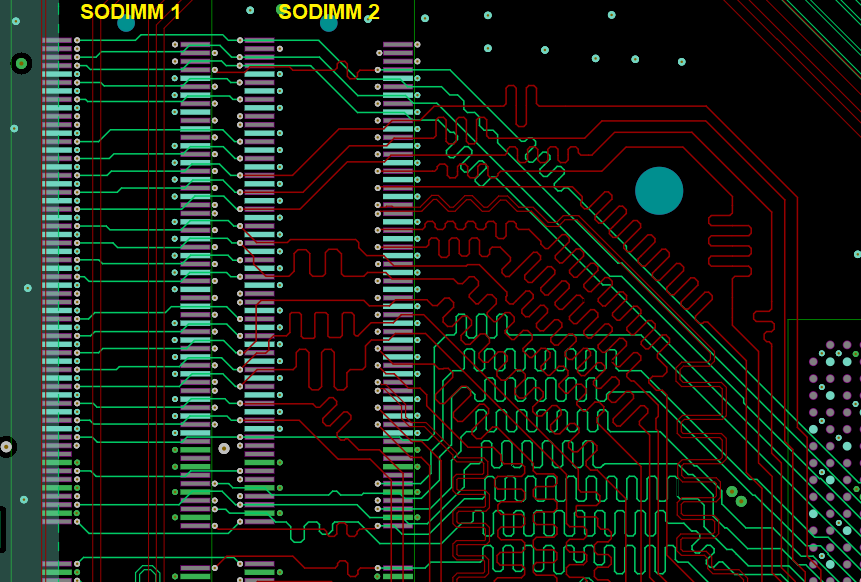
Using SDRAM Vs. DDR RAM In Your PCB Design | Blog | Altium Designer
 resources.altium.com
Using SDRAM vs. DDR RAM in Your PCB Design | Blog | Altium Designer
Some LVDS PCB Layout Guidelines For Ensuring Signal, 40% OFF
 www.oceanproperty.co.th
Some LVDS PCB Layout Guidelines For Ensuring Signal, 40% OFF
Main Design Guidelines & Layout Rules On High Speed PCB
 www.integrasources.com
Main Design Guidelines & Layout Rules on High Speed PCB
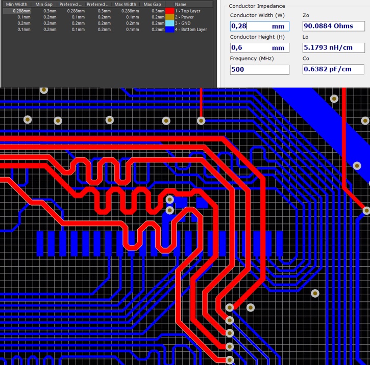
Pcb Design Differential Impedance Of Lvds Rules And T - Vrogue.co
 www.vrogue.co
Pcb Design Differential Impedance Of Lvds Rules And T - vrogue.co
PCB Layout Guidelines For Decoupling And Bypassing Capacitors
 www.onelectrontech.com
PCB Layout Guidelines for Decoupling and Bypassing Capacitors ...
PCB Design Tutorial: Basic Rules, Tips And Guidelines-TechSparks
 www.tech-sparks.com
PCB Design Tutorial: Basic Rules, Tips and Guidelines-TechSparks
24. top 5 pcb design guidelines every pcb designer needs to know,pcb design. Some lvds pcb layout guidelines for ensuring signal integrity. lvds-pcb-layout-guidelines für gute signalintegrität